Product
DAC DAC(Digital to Analog Convertor)
Introduction
Having continued to grow as a manufacturer of weighing and measuring instruments, A&D is now going further with active challenges to up-and-coming businesses using unique technological skills accumulated over almost three decades.
In recent years, A&D has especially focused on A/D and D/A conversion devices and electron beam businesses supporting semiconductor development.
Offering Miniaturization Technologies for Semiconductor Processing and Controlling
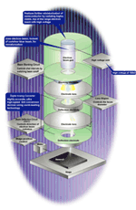 Semiconductor integrated circuits such as microprocessors and computer memories are constantly required to offer more capacity and to achieve further miniaturization. For this reason, light source used in lithography is shifting toward an electron beam radiated from an electron gun with a shorter wavelength than that of the common laser beam. A&D started developing electron guns early on and successfully developed those offering top of the range high voltage output and excellent stability operation rate. In addition, this technology has prospects for use in DVD mastering and is currently used with ion guns for surface analysis.
Furthermore, A&D has the advantage having developed peripheral circuitries to control electron beam. The A/D and D/A conversion technologies that A&D is extremely proud of are currently applied to ultra high-speed, highly accurate D/A converters (DAC) for beam deflection circuits to control the direction of electron beam radiation. A&D's blanking circuits for controlling beam radiation intervals and lens aligner for controlling beam diameter, etc. are also highly recommended by professionals in the industry.
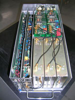
DAC Business
DAC requirements are becoming tougher and tougher due to ongoing competition in the miniaturization of semiconductors. An example of this is A&D's ±320V output with 20-bit accuracy at 10µS stabilization time. The contradicting factors of accuracy and speed are a major issue because the positioning error of an electron beam affects pattern writing accuracy but high-speed performance is required to increase throughput.
A) Main deflection amplifier Specifications
Model AD-199-5
| Output voltage | ±400V max |
|---|---|
| Settling Time | 60 µS (Full Swing) |
| Resolution | 18-bit |
| Linearity | ±1/2LSB (17-bit) |
| Temperature Coefficient | < ±8ppm/2°C, 1 hr |
| Noise | < ±1LSB |
B) Sub deflection amplifier Specifications
Model AD-199-3
| Output voltage | ±37.5V max. (POS, NEG) |
|---|---|
| Settling Time | 50 nS less |
| Resolution | 12-bit |
| Linearity | ±1/2LSB (12-bit) |
| Temperature Coefficient | < ±100ppm/2°C, 1 hr |
| Noise | < ±1LSB |
| Permissible Load | < 30 PF |
| Output Offset | Within ±3.2% of FS |
C) Lens and Aligner Specifications
Lens out : 4 ch
| Output Current | ±2 A |
|---|---|
| Stability | < ±1ppm |
Lens out : 4 ch
| Output Current | ±2 A |
|---|---|
| Stability | < ±10ppm |