Semiconductor engineer Gordon Moore, co-founder of Intel, first observed an interesting relation in 1964 about the development of semiconductor technology. He mentioned, "The logic density of silicon integrated circuits has closely followed the curve (bits per square inch) = 2 to (t - 1962)th power where "t" is time in years." That is to say the power of an IC chip will be doubled each year starting from 1962. His observation became a prediction, then a law or norm, which the semiconductor industry has to follow, and it is now known as Moore's Law, and which really makes semiconductor engineers paranoid if they are off-track.
As we all know very well, memory chips have been increasing in capability and capacity each year while the price has been decreasing. According to the findings, the trend has followed Gordon Moore's observation literally until the late 1970's. Since the late 1970's, the doubling period has slowed to 18 months and remains true today. If you use these after the facts, the formula becomes 2 to the 27th power or the logic density has increased by 130 million times since 1962. With this calculation a 2 byte memory chip in 1962 has become a 260 megabyte memory chip in 2000, which sounds amazingly close to the fact (256 megabyte chips).
The semiconductor or IC chip fabrication process is, in a crude sense, similar to photo etching and printing. You print a pattern on a silicon wafer and photo-etch it and you repeat this process to create a great number of transistors on the wafer. (That is why it is referred to as lithography). Therefore, what Moore's Law says is each year the patterns or lines created on the silicon wafer get finer or narrower so you can have more transistors on the same area of silicon wafer. Since the width and the area has a relation of squares, in order to increase a density by 2 the width of the lines has to decrease by a square root of 2 or 1.4 times.
In the late 1970's, there was a lot of hot discussion as to the limits of the photo etching based semiconductor production, as light behaves like a wave which results in blurring; and how sharp or fine patterns will be related to the wavelengths of light used for the process. The diffraction of light imposes limits on this technology. (For instance a visible light of red has a wavelength of 7000 Angstrom, 0.7 micrometers or 700 nanometers, and with this light you cannot avoid blurring in the magnitude of 0.7 micrometer).* Thus, a great amount of research money has gone to new process developments involving beams other than light. Heavy particles are natural choices because they have very little diffraction. (Quantum physics tells us even particles have wave characteristics. They have blurring like light, but the blurring is negligible compared to light, thus we don't see such behavior when we throw a ball). Other substitute candidates for light that were seriously investigated among were electrons and ions.
If you recall "Hidden Business for A&D," written by Masayuki Kogure in July 1998 (refer to the July 1998 Issue of Marketing UpDate), A&D has participated in developing the next generation semiconductor equipment since the founding of our company. Our part was to develop electronics or circuitry to control electron beams. With the conventional process, the lenses are the essential components to control light, but when electron beams are used, you have to use magnetic or electrical forces to control beams instead of lenses. The unprecedented precision and speed in terms of fine-tuning and positioning the electron beams have become the key elements in the circuitry development. Mr. Ikehata, who is in charge of digital-to-analog converter development for this equipment, says the precision is like positioning a beam by 50 cm increments between Tokyo and Osaka or 550km in distance at a speed of 3/1,000,000 of a second.
The semiconductor history took a strange turn in the late 1970's. Contrary to the common prediction then, photo etching or lithography technology kept improving and survived to live up to Moore's Law. Our circuitry technology then developed for electron beam lithography was put on the backburner for more than 10 years. A team of our engineers who excelled in analog circuitry designs were dispersed and assigned to different jobs, in spite of their desire and ambition to provide the world's best circuitry for the next generation electron beam lithography.
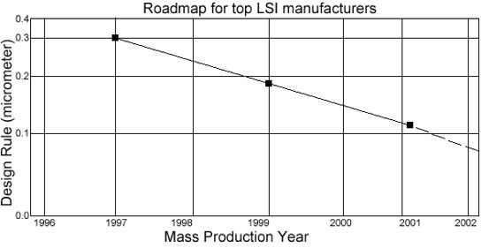
Recently the situation has changed drastically. The design rule for chips in recent years is quickly approaching 100nm or 0.1 micrometer (See the chart below), and this time is definitely nearing the physical limitations of light. Electron beam lithography has come back!
When you hold a mobile phone equipped with a digital camera or any other wide-band wireless communication tool, you may be using chips with less than a 100-nanometerdesign rule. A&D continues to support this technology through our old, yet still, state of the art analog technology, which we have stubbornly kept and nurtured in-house.
It is also nice to realize that not only are we helping Moore's Law continue to be viable for a few decades to come, but we are also bringing analog engineers or those once considered to be old timers back to the main stage.
*Note) The state of the art photo lithography uses a Krypton Fluoride (KrF) laser beam which has a wavelength of 248 nanometers or Argon Flouride (ArF) laser beam which has a wavelength of 193 nanometers.
You may address any comments concerning this editorial by email to Mr. Eto